|
|
|
The Display Description Small Story The Power Supply Logic part Connection to I²C Bus The Border
To Gallery The PCB's The technical part The Software
|
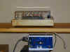
Author: Udo Sobotta Target of Project: SC12@Chip The Display
Nixie - root: ancient Germanic
Nixies are ghosts, who live mostly in their element - the water. The male Nixie was never seen before. The female Nixie could be observed several times while taking a sunbath. If a human being could catch a glimpse on those beautiful creatures, it might happen, that he goes out of his mind. Back to technology A project like this I had in my mind for a long time. The reason why is simple: I bought 18 of those Nixie® Tubes, very cheap during Hobbytronic in Dortmund. After that I was searching for a good reason to utilise them. While starting up, building and programming the SC12, I got opportunity to understand the serial I²C Bus better while creating a Display. Since I'm an absolute fan of Clocks with a rare or special display the idea to use those Nixie® Tubes to create a new clock for my Desk, was born. Short hand decission. Put three in one, create a nice case, develop the hardware and create the Software to make it run. This Idea should come true during the rainseason, Novemver 2001. While this project was an 'add on' to my normal work and education I had to find a gap in order to realise my Ideas. I modified the definition of my daily workload/freetime – and – I re-defined the day to a total amount of 25 hours. If this wouldn't be enough, I still may use the left over night. (Many thanks to Mr. Günzel – Mentor in mathematics – for this very useful tip). Sounds easy - in practice: It was a huge amount of additional work. Despite the time spend for the Hardware development my left over time was decreased while I tried to use a recommended tool out of Microsoft
Windows™ world. This time consuming tool carries the name Frontpage and insist to be a Web-editor. I tried to use this tool to realise the Web access interface
for the calendarium and the web basing control System for my Software. My trial failed 100%. Description of Project The System is basically divided into three parts:
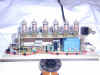
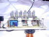
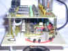
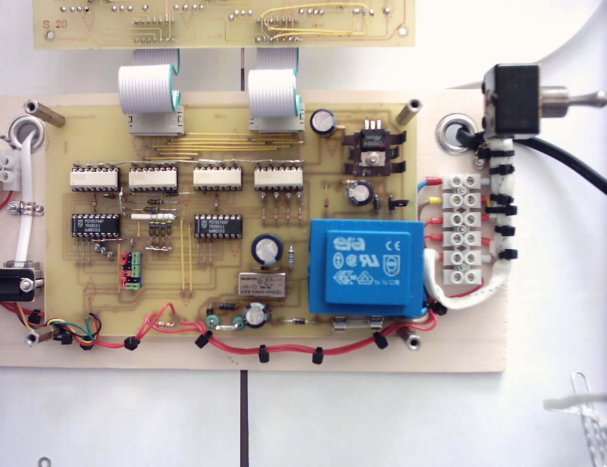
The Power Supply a standard one. Starting from a 12V AC source using rectfying diodes(2-4) and a capacitor (C4) we get an outgoing voltage of 14 Volt DC. Followed by a DC 5V stabiliser IC. I created the supply for all IC(1-8). Every IC need a capacitor to block the incoming power. The DC 5V high, I name this part of incoming power High, because of it's direct connection to Main Power Line using the Jumper. !! Caution!! Open the Jumper as long as you are performing your tests within the normal Logic. Better: Use a transformer (AC240V-AC240V). Remember always: it's the only one live you have!! I don't want attent your funeral. To make things easy I generated the high Voltage for the Anodes directly out of the Main Power Line. Diode D1 rectifies one halfwave
of the main power line into a high voltage stable electrolytic capacitor(C3). Every positive halfwave charges the capacitor.
After a few time the capacitor reaches an average Voltage of 160 to 170 Volt. This is too high to drive the Tubes, but how to reduce the Voltage to 140 Volt? I use the classic
Z-Diode principle for stabilisation of the Anode Power. Since I didn't had a single Z-Diode of the requested 140V Type, I used two Z-Diodes (D6/D7) of 68 Volt in series. I am slightly
below the recommended Values, but still within the tolerances. The resistor(R2) must be able to 'consume' 1.3 Watt. I selected a 5 Watt type in order to get a larger surface.
(larger surface = lower outside temperature) The resistor R3 is a (parallel) pre Resistor which changes it's value due to the connected LDR. This 'trick' allows the Display to dimm
down, when the environmental light is less and to go to full lightning capacity during daytime. The last part of the power supply: The Relais Re 1. This Relais is necessary, if a ‚single’ Power supply for High and Low Voltage is in use this is because of – if the LV Powered parts getting their power later than the HV is supplied, this might cause problems or even damages to the Nixie® Dirver IC's. Therefore C5 will be charged using the the Resistor (Rx). After short delay, the Relais switches the HV onto the circuits. Opposite to Power on, during Power off, the Relais remains in ON Condition even after the HV is already discharged using the energy of the capacitor. After few delaytime (depending in τ=R*C) the relay switches off. This is protecting the sensitive Nixie® Driver IC. Always: Logicpart before Powerpart. The Displaydriver and Logic part receive their power from the DC 5VHigh power supply.
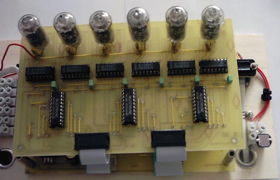
All Nixie® Driver are receiving a binary coded signal and decode it into a decimal output.
Counting from 0 to 9 request 4 Bit. Therefore we need 4 data lines for each Digit (Hour, Minute, Second in tens and single digit). Four wire per Driver will result in 24 wire for the 6 digit display. Knowing I have two 8 bit driver I thought myself: "Too many, I have to
reduce the data lines.". I²C Bus utilisation Signals have to control the Display. Where are they coming from? The SC12@chip is the control circuit. Or even better: the I²C Port IC. To control 8 Data and 3(4) Controllines we need to utilise two 8 Bit control IC. One IC controls the data, the second for the Latch enable signals. Why? - wouldn't be one IC enough? - Theoretically yes, when multiplexing the High/Lowbyte. But the Control IC may set all output at same time only - how to select between Data, Enable and Multiplex signals? Once the Data Signal is stable, how to switch on the Enable signals and when shall the multiplexing take place? This requires at least more IC's and a lot of programming work more. How to sabilise the Software control? Does it worth? No - I decided to use two IC: one for the Data and one for the controls! However, Data and enable signals are now available. Any other problem? Oh - the Latches are, as you may remember somehow connected to 240V Main Power Line. Should the SC12@Chip be connected in same way? No, we need to separate the Logic and the Display part. The I²C Port IC are the best place to do this. The Data / Control signals from I²C IC's will control the LED in a Optocoupler. Now we may touch the SC12@Chip and the logic. All other parts in contact to the Display tubes are connected to Main power line. Are we now safe? Yes we are. Take a short spot to the Circuit diagram. Top right side you may see the function of an Photocoupler. If the LED is emitting light, the Phototransistor turns down to Zero Ω. Once the LED turns off, the resistance becomes infinite. We're done. The galvanic isolation Now it's time to step over this border. The second part of the Opto coupler contains the LED and a serial resistor(16). Those resistors are connected to incoming DC 5V of the I²C Bus provided from our SC12@chip. This line is the power source for the I²C Port IC too. However, the input of the Opto's will be connected to the outputs of the I²C Control IC. The moment the Output is switched ON, the LED becomes energised and is emitting light to the Photo Transistor. The Photo transistor was part of last Chapter. Both Port IC need to have different Addresses. This may be set in the program and has to be set in the external Jumperfield. The visible Jumper field contains the complete range of addreses. To reduce cost, one or two short circuit wire may do the same, but what about the "View"? The Nixie® Driver IC5,6 and the Latch IC16 aren't mentioned, but they are a perfect copy of the others - except the 3rd address wire.
|
|
|
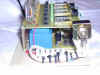
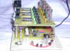
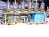
Please click on the relevant Picture to get the full screen Version.
|
|
|
PCB and other Diagrams The PCB layout are ready for download in PDF format. Use the Adobe Acrobat Reader to show and to print them. Use A4 as standard setting for best results.
Download PCB Layout
Display
Controls Download Plans / BOM Display_Components Control_Components Bill of Material BOM Link to SC12 SC12@Chip |
|
|
Here you may download a I²C Test Program.
this program detects the actual amouont of I²C components attached to the Bus. |
|
DCF 77 Program |
Here you may download the DCF77_Nixie_CGI_Display Program.
This program has been written especially for this Project. It fulfils the requests given by mentor. It contains the original Nixie driver program as well
as the Web extension as CGI and the full support to decode the DCF77 Signal. After starting this program, the SC12@Chip synchonizes to actual time using DCF signals.
The generated Webpage shows the time of last Synchronisation as well as the actual date on the Calendar.
Additional we may set a date or time to see the Calendar sheet of this particular month. Since the RTC of the SC12@Chip is very sensitive in terms of power cuts,
my one loses date and time, I implemented the function of Year '1' to stop the running program using the Web Interface. |
|
Since my point of interest has moved to Linux and Server Programming, I dropped the Project to create an NTP server.
The SC12@Chip became an NTP-Client to my Linux Superserver. |
|
| © Udo Sobotta | Last update 15.09.2009 |


